
المزايا الأساسية
✅ Nanometer‑Level Precision
Flatness ≤0.005mm, surface roughness Ra≤0.1μm, ideal for wafer transfer & lithography alignment.
✅ Extreme Environment Resistance
Operating temp 800–1600°C; plasma & acid/alkali resistant (pH 1–14); service life ×5+ vs metal.
✅ Ultra-High Cleanliness
Metal ion leaching ≤1ppm; no particle shedding (NAS 1638 Class 1); EUV & high-purity process compatible.
✅ Excellent Thermal Management
AlN thermal conductivity ≥170W/m·K; CTE matches silicon (4.5×10⁻⁶/℃), reduces thermal stress.
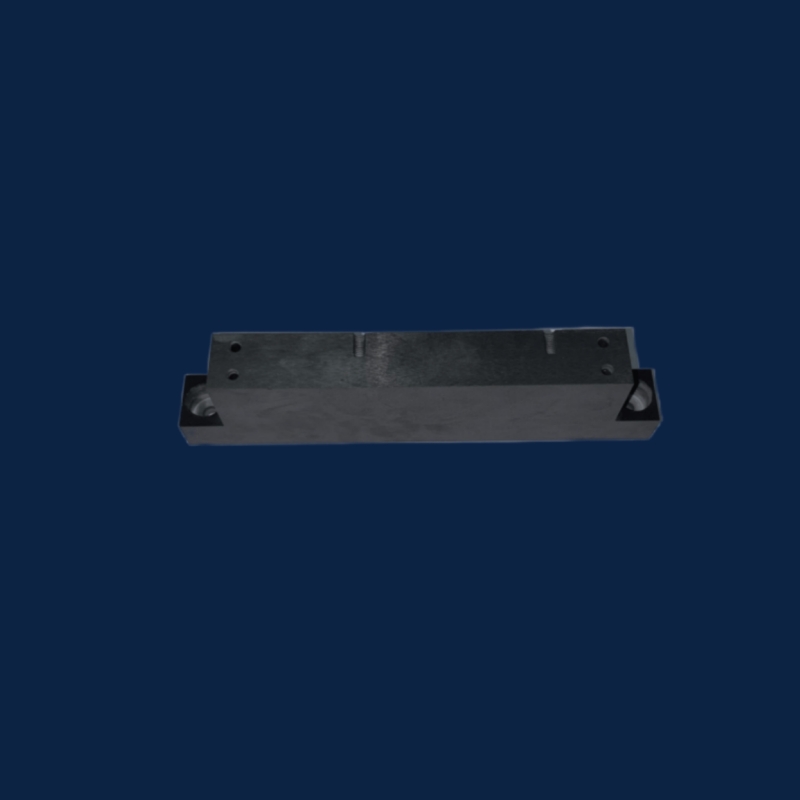
التطبيقات النموذجية & Material Selection
Wafer Handling & يدعم
Wafer Chuck: آل₂O₃(99.5%) / كربيد كربيد(99.9%); flatness ≤0.003mm; electrostatic force ≥0.1MPa.
Vacuum Chamber Flange: آل ن; hermeticity ≤1×10⁻⁹ Pa·m³/s.
Gas Distribution & Reaction Control
Gas Distribution Plate: YSZ (plasma resistant); pore tolerance ±0.005mm.
Heater Base: كربيد كربيد; temp resistance 1600°C; resistance uniformity ≤±1%.
Lithography & Inspection
EUV Optic Holder: Invar alloy (ultra-low CTE).
Wafer Alignment Stage: AlSiC; positioning repeatability ≤±10nm.
Our Service Strengths
Full customization: material selection, precision grinding, CVD coating.
Functional integration: embedded electrodes & sensors.
Cost advantage: 30–50% lower than imported brands.


