 جيفينج سيراميك

مع التطور السريع للصناعات مثل الذكاء الاصطناعي (منظمة العفو الدولية), الحوسبة عالية الأداء (HPC), مركبات الطاقة الجديدة والتغليف المتقدم, يتجه تصنيع أشباه الموصلات العالمي نحو تقنيات المعالجة الأعلى, عوائد أعلى ومتطلبات نظافة أكثر صرامة. من معالجة الرقاقات إلى تغليف الرقائق, تحتاج معدات أشباه الموصلات إلى العمل بشكل مستمر في درجات حرارة عالية, فراغ عالية, تآكل قوي, البلازما والبيئات فائقة النظافة, مما يضع متطلبات عالية للغاية على أداء مكونات المعدات.
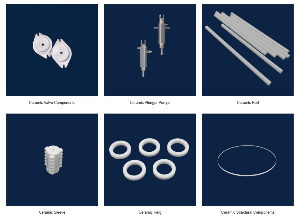
على الرغم من أن المواد المعدنية التقليدية تتمتع بقوة ميكانيكية ممتازة, لديهم قيود معينة من حيث مقاومة التآكل, أداء العزل الكهربائي, مقاومة تآكل البلازما, والتحكم في الجسيمات. لذلك, يتم الآن تصنيع المزيد والمزيد من المكونات الرئيسية باستخدام السيراميك الصناعي الدقيق.
في الوقت الحاضر, السيراميك المتقدم أشياء مثل الألومينا, كربيد السيليكون, نيتريد الألومنيوم, ويتم استخدام نيتريد السيليكون على نطاق واسع جدًا في آلات الحفر , معدات الأمراض القلبية الوعائية, معدات PVD, أنظمة معالجة الرقائق, وأجهزة التفتيش. إنهم يلعبون بطريقة ما دورًا حاسمًا في الحفاظ على تشغيل الترس بثبات وفي زيادة إنتاجية الرقاقة.
لماذا تعتبر المكونات الخزفية الدقيقة ضرورية في معدات أشباه الموصلات?
يتطلب تصنيع أشباه الموصلات متطلبات بيئية عالية للغاية, المطالبة بدرجات حرارة عالية, تآكل قوي, مجالات كهربائية قوية, ونظافة فائقة. يظل السيراميك هو المادة الأكثر ملاءمة.
بالمقارنة مع المواد المعدنية التقليدية, السيراميك المتقدم له المزايا التالية.
درجة نقاء عالية, تقليل مخاطر التلوث
يتطلب تصنيع أشباه الموصلات رقابة صارمة للغاية على الشوائب. مواد سيراميكية عالية النقاء مثل الألومينا, كوارتز, ونيتريد الألومنيوم يمكن أن يقلل بشكل فعال من تلوث أيونات المعادن ويقلل من إطلاق الجسيمات, مما يساعد على تحسين إنتاجية الرقاقة.
أداء ممتاز لمقاومة درجات الحرارة العالية
عمليات مثل الانتشار, أكسدة, وتتطلب الأمراض القلبية الوعائية عادةً بيئات عمل تبلغ درجة حرارتها عدة مئات أو حتى آلاف الدرجات المئوية. يتمتع السيراميك المتقدم بمقاومة ممتازة للحرارة ويمكنه الحفاظ على ثبات حجمه وقوته الميكانيكية في درجات حرارة عالية دون التعرض للتشوه.
مقاومة متميزة للتآكل الكيميائي
يجب أن تتلامس معدات أشباه الموصلات على المدى الطويل مع الفلوريدات, الكلوريدات ومختلف الغازات القوية المسببة للتآكل. بالمقارنة مع المعادن, يتمتع السيراميك بمقاومة أفضل للتآكل ويمكنه إطالة عمر خدمة المكونات بشكل فعال.
مقاومة جيدة لتآكل البلازما
أثناء عمليات حفر البلازما وترسيب الأفلام, تتعرض المعدات باستمرار للبلازما عالية الطاقة. يمكن لمواد مثل كربيد السيليكون وأكسيد الألومنيوم أن تقاوم تآكل البلازما بشكل فعال, تقليل انفصال الجسيمات, وتعزيز استقرار المعدات.
أداء عزل كهربائي ممتاز
تتطلب العديد من أجهزة أشباه الموصلات تحكمًا دقيقًا في المجالات الكهربائية ذات الجهد العالي والتردد العالي. يمتلك السيراميك مثل الألومينا ونيتريد الألومنيوم خصائص عزل كهربائي ممتازة, والتي يمكن أن تمنع بشكل فعال مشاكل مثل التسرب والتفريغ.
المواد الخزفية الشائعة المستخدمة في تصنيع أشباه الموصلات
| مواد | الميزة الرئيسية | نقاء نموذجي | الميزات الرئيسية | سيناريوهات التطبيق النموذجية |
| آل₂O₃ – أكسيد الألومنيوم | تكلفة منخفضة, عزل ممتاز, مقاومة للاهتراء | 99.5% – 99.9% | صلابة عالية, خسارة عازلة منخفضة | الدعم الهيكلي, كؤوس الشفط, حلقات عازلة |
| آل ن – نيتريد الألومنيوم | الموصلية الحرارية العالية, العزل الكهربائي | زيادة 99% | الموصلية الحرارية أعلى من 170 وات/م·ك | لوحة تسخين تشاك كهرباء |
| كربيد كربيد – كربيد السيليكون | مقاومة للغاية لتآكل البلازما | تلبد رد فعل عالي النقاء | صلابة عالية, مقاومة لقصف البلازما | حلقة التركيز, لوحة الرش, بطانة التجويف |
| زرو₂ – أكسيد الزركونيوم | صلابة عالية, قوة عالية | 3Y-TZP | صلابة عالية للكسر | المكونات الهيكلية الميكانيكية, دبابيس تحديد المواقع |
| Si₃N₄ – نيتريد السيليكون | قوة عالية, مقاومة للاهتراء, خفيفة الوزن | درجة نقاء عالية | أداء ممتاز للصدمات الحرارية | محامل, مكونات ذراع النقل |
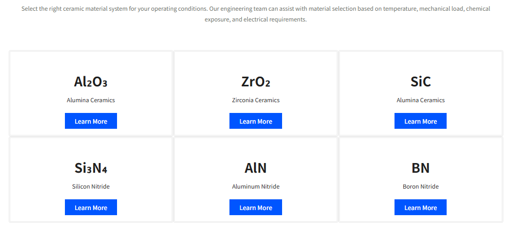
يعتمد اختيار مادة السيراميك المناسبة على درجة حرارة التشغيل, التعرض للبلازما, متطلبات العزل الكهربائي, والقوة الميكانيكية. مختلف مواد السيراميك التقنية مناسبة لتطبيقات أشباه الموصلات المختلفة. تعتبر مادة الألومينا هذه هي المادة الأكثر استخدامًا على نطاق واسع نظرًا لفعاليتها العالية من حيث التكلفة; يتمتع كربيد السيليكون بمزايا كبيرة في عمليات الحفر; ونيتريد الألومنيوم يهيمن على مكونات الإدارة الحرارية.
مكونات السيراميك النموذجية في معدات أشباه الموصلات
يتم استخدام السيراميك المتقدم في جميع معدات تصنيع أشباه الموصلات الأساسية تقريبًا.
- معدات النقش
يستخدم للمكونات الرئيسية مثل حلقة التركيز, حلقة الدرع, و إي إس سي, لضمان التشغيل المستقر لعمليات البلازما. - معدات الأمراض القلبية الوعائية
يتم تطبيقه على أنظمة توزيع الغاز, بطانات التجويف, مكونات عازلة, إلخ. - معدات PVD
يستخدم لعزل مكونات الدعم والأجزاء المقاومة للحرارة العالية, لتعزيز الاستقرار التشغيلي للمعدات. - معدات فحص الرقاقة
يستخدم منصة سيراميك عالية الدقة وأكواب شفط لتعزيز دقة الفحص. - نظام التعامل مع الرقاقة
عدد كبير من المكونات مثل الأيدي الميكانيكية, القضبان, وأكواب الشفط مصنوعة من مواد السيراميك, الحد من تلوث الجسيمات. - معدات المعالجة الحرارية
يمكن لقوارب الكوارتز والدعامات الخزفية في المعدات مثل أفران الانتشار وأفران الأكسدة أن تتحمل درجات الحرارة العالية لفترة طويلة.
كيفية اختيار المكونات الخزفية الدقيقة لمعدات أشباه الموصلات?
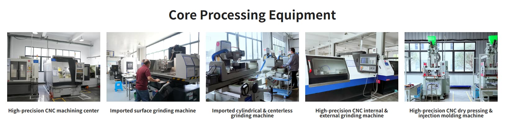
لمصنعي المعدات, إن اختيار مكونات السيراميك لا يتطلب التركيز فقط على المادة نفسها, ولكن أيضًا النظر بشكل شامل في قدرات المعالجة ومستويات مراقبة الجودة. إن اختيار مورد موثوق لا يقل أهمية عن اختيار المادة المناسبة. تقنية جيفينج مع الإمكانات الداخلية الكاملة - يمكن أن توفر اتساقًا أفضل وتفاوتات أكثر صرامة.
نقاء المادة
يمكن للمواد عالية النقاء أن تقلل من إطلاق الشوائب وتقلل من خطر تلوث الرقائق.
دقة المعالجة
تتطلب معدات أشباه الموصلات عادةً تسامحًا وتسطيحًا للأبعاد على مستوى الميكرون, لذلك يحتاج الموردون إلى امتلاك طحن عالي الدقة, قدرات التلميع والمعالجة الدقيقة.
جودة السطح
خشونة السطح الممتازة يمكن أن تقلل من توليد الجزيئات وتعزز استقرار المعدات.
أداء مقاومة البلازما
لمعدات النقش, وينبغي أن يكون التركيز على مقاومة المادة لتآكل البلازما لإطالة عمر المكونات.
القدرة على التخصيص
تختلف هياكل المعدات المختلفة بشكل كبير. الموردين الذين يمكنهم تقديم التخصيص غير القياسي, معالجة الهياكل المعقدة, والتسليم السريع لها ميزة تنافسية أكبر.
اتجاهات تطوير السيراميك الدقيق لأشباه الموصلات
مع التطوير المستمر لعمليات 3nm و2nm المتقدمة وتقنيات التعبئة والتغليف المتقدمة, تضع معدات أشباه الموصلات متطلبات أعلى على المواد الخزفية.
في المستقبل, درجة نقاء عالية, انخفاض حجم الجسيمات, مقاومة عالية للبلازما, الموصلية الحرارية العالية, وسوف تصبح دقة الأبعاد الأعلى هي اتجاه تطوير السيراميك الدقيق. في نفس الوقت, من المتوقع أن تستمر نسبة تطبيق السيراميك عالي الأداء مثل كربيد السيليكون ونيتريد الألومنيوم في الزيادة لتلبية متطلبات الموثوقية واستقرار العملية لمعدات أشباه الموصلات من الجيل التالي.
بالإضافة إلى, مع استمرار صناعة أشباه الموصلات العالمية في التوسع, يميل مصنعو المعدات بشكل متزايد إلى اختيار موردي مكونات السيراميك الشاملين الذين يتمتعون بقدرات في مجال البحث والتطوير في المواد, الآلات الدقيقة, والتصنيع المخصص لتقصير دورات التطوير وضمان استقرار سلسلة التوريد.
خاتمة
في صناعة أشباه الموصلات, لا تعد مكونات السيراميك الدقيقة من المعدات المهمة فحسب، ولكنها تؤثر أيضًا بشكل مباشر على دقة المعالجة, استقرار المعدات, والعائد رقاقة. بدءًا من الخراطيش الكهروستاتيكية وحلقات التركيز وحتى مكونات معالجة الرقاقات, السيراميك المتقدم المختلفة, بفضل مقاومتها الممتازة لدرجات الحرارة العالية, مقاومة التآكل, مقاومة البلازما, وخصائص العزل الكهربائي, أصبحت مواد أساسية لا يمكن الاستغناء عنها في معدات أشباه الموصلات الحديثة.
لمصنعي المعدات وشركات الشراء, اختيار المواد الخزفية المناسبة, تقنيات المعالجة الناضجة, ولا يستطيع الموردون الذين يتمتعون بقدرات تصنيع عالية الدقة تحسين أداء المعدات فحسب، بل يمكنهم أيضًا تقليل تكاليف الصيانة, توفير دعم فني أكثر موثوقية لتصنيع أشباه الموصلات المتقدمة.
