 جيفينج سيراميك

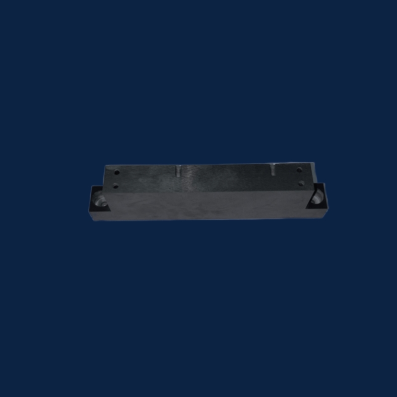
Core Advantages Of Ceramic مكونات معدات أشباه الموصلات
Nanometer‑Level Precision
Flatness ≤0.005mm, خشونة السطح Ra<0.1μm, ideal for wafer transfer & lithography alignment.
مقاومة البيئة القصوى
درجة حرارة التشغيل 800-1600 درجة مئوية; plasma & مقاومة للأحماض/القلويات (الرقم الهيدروجيني 1-14); service life ×5+ vs metal.
Ultra-High Cleanliness
Metal ion leaching ≤1ppm; لا ذرف الجسيمات (NAS 1638 فصل 1); EUV & high-purity process compatible.
Excellent Thermal Management
AlN thermal conductivity ≥170W/m·K; CTE matches silicon (4.5×10⁻⁶/℃), reduces thermal stress.
التطبيقات النموذجية & Material Selection
1. Wafer Transport & يدعم
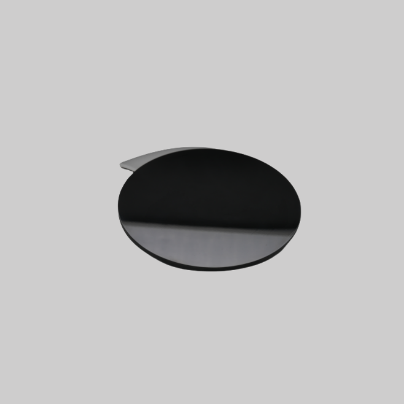
ويفر تشاك
أداء: Electrostatic adsorption force ≥0.1MPa, flatness ≤0.003mm, compatible with thinning and bonding of 12-inch wafers.
Vacuum Chamber Flange
أداء: Gas tightness ≤1×10⁻⁹ Pa·m³/s, suitable for etching and PVD equipment.
2. Gas Distribution & Reaction Control
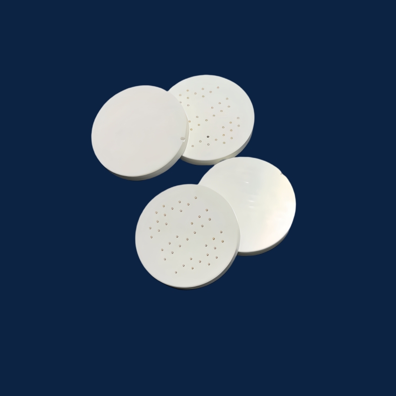
Gas Distribution Plate
أداء: Micropore diameter tolerance ±0.005mm, uniformity error ±2%.
Heater Base
أداء: Resistance uniformity ≤±1%, designed for MOCVD epitaxial growth.
3. الطباعة الحجرية & Inspection Equipment
EUV Optical Lens Base
أداء: Thermal stability ±0.01μm/°C, compatible with processes below 7nm.
Wafer Alignment Stage
أداء: Repeat positioning accuracy ±10nm, matches lithography focusing systems.
Why Partner with JiFeng Ceramics?
Material Selection
الألومينا / نيتريد الألومنيوم / كربيد السيليكون / Special Alloys, compatible with diverse semiconductor process requirements.
تحسين العملية
Precision grinding (tolerance ±0.001mm) and CVD coating for superior wear and plasma resistance.
التكامل الوظيفي
Embedded electrodes and sensors, matching intelligent temperature control and real-time monitoring systems.
ميزة التكلفة
Adopts domestic high-purity powder and machining technologies, بأسعار أقل بنسبة 30% إلى 50% من العلامات التجارية المستوردة.