 JiFeng Ceramics

With the rapid development of industries such as artificial intelligence (AI), high-performance computing (HPC), new energy vehicles and advanced packaging, global semiconductor manufacturing is moving towards higher process technologies, higher yields and stricter cleanliness requirements. From wafer processing to chip packaging, semiconductor equipment needs to operate continuously in high-temperature, high-vacuum, strong corrosion, plasma and ultra-clean environments, which places extremely high demands on the performance of equipment components.
Although traditional metal materials have excellent mechanical strength, they have certain limitations in terms of corrosion resistance, electrical insulation performance, resistance to plasma erosion, and particle control. Therefore, more and more key components are now being manufactured using precision industrial ceramics.
Nowadays, advanced ceramic stuff like alumina, silicon carbide, aluminum nitride, and silicon nitride are being used pretty widely in etching machines , CVD equipment, PVD equipment, wafer handling systems, and inspection devices. They somehow play a crucial role in keeping the gear running stably and in raising the chip yield.
Why Are Precision Ceramic Components Essential in Semiconductor Equipment?
Semiconductor manufacturing has extremely high environmental requirements, demanding high temperatures, strong corrosion, strong electric fields, and ultra-high cleanliness. Ceramics remain the most suitable material.
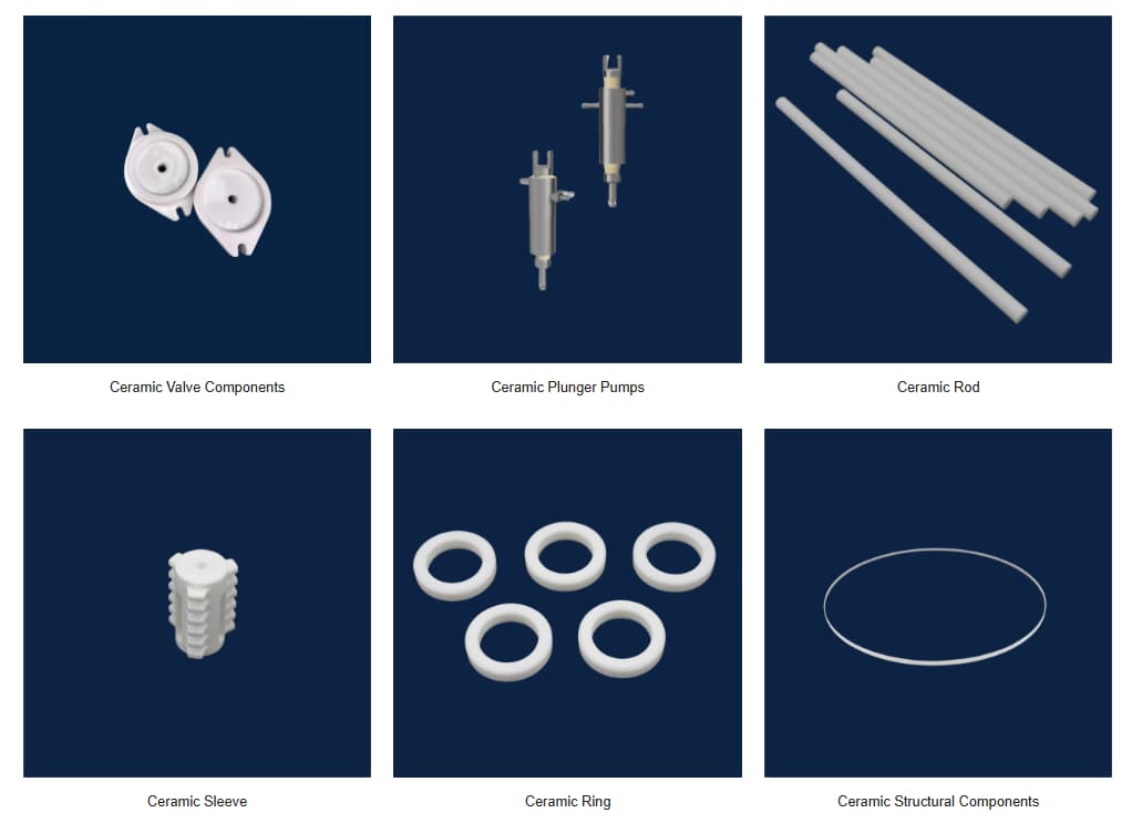
Compared to traditional metal materials, advanced ceramics have the following advantages.
High purity, reduced pollution risk
Semiconductor manufacturing requires extremely strict control over impurities. High-purity ceramic materials such as alumina, quartz, and aluminum nitride can effectively reduce metal ion contamination and decrease particle release, which helps to improve wafer yield.
Excellent high-temperature resistance performance
Processes such as diffusion, oxidation, and CVD usually require working environments of several hundred or even thousands of degrees Celsius. Advanced ceramics have excellent heat resistance and can maintain their size stability and mechanical strength at high temperatures without undergoing deformation.
Outstanding resistance to chemical corrosion
Semiconductor equipment needs to come into long-term contact with fluorides, chlorides and various strong corrosive process gases. Compared to metals, ceramics have better corrosion resistance and can effectively extend the service life of components.
Good resistance to plasma erosion
During the plasma etching and film deposition processes, the equipment is constantly exposed to high-energy plasma. Materials such as silicon carbide and aluminum oxide can effectively resist plasma erosion, reduce particle detachment, and enhance the stability of the equipment.
Excellent electrical insulation performance
Many semiconductor devices require precise control of high-voltage and high-frequency electric fields. Ceramics such as alumina and aluminum nitride possess excellent electrical insulation properties, which can effectively prevent problems such as leakage and discharge.
Common Ceramic Materials Used in Semiconductor Manufacturing
| Materials | Main advantage | Typical purity | Key features | Typical application scenarios |
| Al₂O₃ – Aluminum Oxide | Low cost, excellent insulation, wear-resistant | 99.5% – 99.9% | High hardness, low dielectric loss | Structural support, suction cups, insulating rings |
| AlN – Nitride of Aluminum | High thermal conductivity, electrical insulation | Over 99% | Thermal conductivity above 170W/m·K | Electrostatic chuck heating plate |
| SiC – Silicon Carbide | Extremely resistant to plasma corrosion | High-purity reaction sintering | High hardness, resistant to plasma bombardment | Focusing ring, spray plate, cavity lining |
| ZrO₂ – Zirconium Oxide | High toughness, high strength | 3Y-TZP | High fracture toughness | Mechanical structural components, positioning pins |
| Si₃N₄ – Nitride of Silicon | High strength, wear-resistant, lightweight | High purity | Excellent thermal shock performance | Bearings, transmission arm components |
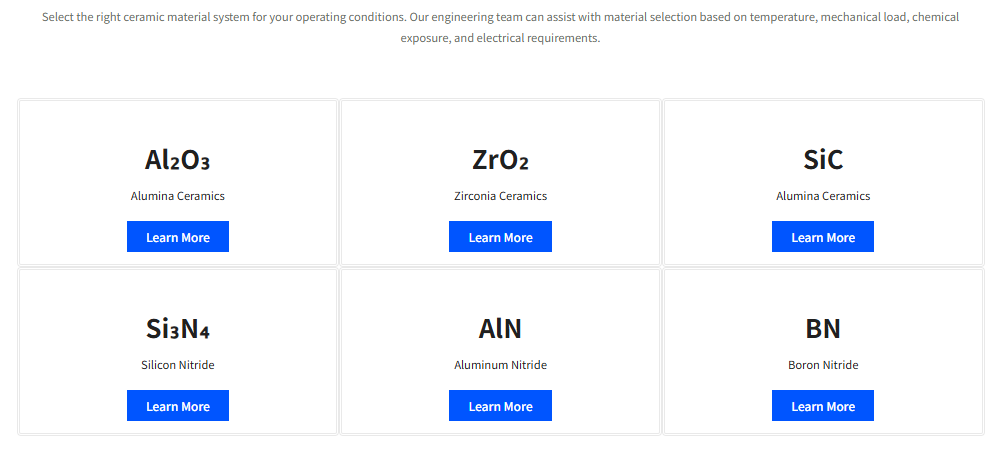
Choosing the right ceramic material depends on operating temperature, plasma exposure, electrical insulation requirements, and mechanical strength. Different technical ceramic materials are suitable for different semiconductor applications. Such us alumina is the most widely used material due to its high cost-effectiveness; silicon carbide has significant advantages in etching processes; and aluminum nitride dominates in thermal management components.
Typical Ceramic Components in Semiconductor Equipment
Advanced ceramics are used in almost all core semiconductor manufacturing equipment.
- Etching equipment
Used for key components such as Focus Ring, Shield Ring, and ESC, to ensure the stable operation of plasma processes. - CVD equipment
Is applied to gas distribution systems, cavity linings, insulating components, etc. - PVD equipment
Used for insulating support components and high-temperature resistant parts, to enhance the operational stability of the equipment. - Wafer inspection equipment
Uses high-precision ceramic platform and suction cups to enhance inspection accuracy. - Wafer handling system
A large number of components such as mechanical hands, rails, and suction cups are made of ceramic materials, reducing particle contamination. - Heat treatment equipment
The quartz boats and ceramic supports in equipment such as diffusion furnaces and oxidation furnaces can withstand high temperatures for a long time.
How to Select Precision Ceramic Components for Semiconductor Equipment?
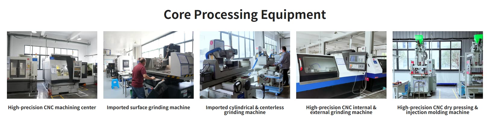
For equipment manufacturers, selecting ceramic components requires not only focusing on the material itself, but also comprehensively considering processing capabilities and quality control levels. Selecting a reliable supplier is just as important as selecting the right material. JiFeng Tech with complete in-house capabilities—can deliver better consistency and tighter tolerances.
Material purity
High-purity materials can reduce the release of impurities and lower the risk of wafer contamination.
Processing accuracy
Semiconductor equipment usually requires micron-level dimensional tolerance and flatness, so suppliers need to possess high-precision grinding, polishing and precision processing capabilities.
Surface quality
Excellent surface roughness can reduce the generation of particles and enhance the stability of the equipment.
Plasma resistance performance
For etching equipment, the focus should be on the material’s resistance to plasma erosion to extend the lifespan of components.
Customization capability
The structures of different equipment vary greatly. Suppliers who can offer non-standard customization, processing of complex structures, and rapid delivery have a greater competitive advantage.
Development Trends of Precision Ceramics for Semiconductors
With the continuous development of advanced 3nm and 2nm processes and advanced packaging technologies, semiconductor equipment places higher demands on ceramic materials.
In the future, high purity, low particle size, high plasma resistance, high thermal conductivity, and higher dimensional accuracy will become the development direction for precision ceramics. At the same time, the application ratio of high-performance ceramics such as silicon carbide and aluminum nitride is expected to continue to increase to meet the reliability and process stability requirements of next-generation semiconductor equipment.
Furthermore, as the global semiconductor industry continues to expand, equipment manufacturers are increasingly inclined to choose one-stop ceramic component suppliers with capabilities in materials research and development, precision machining, and customized manufacturing to shorten development cycles and ensure supply chain stability.
Conclusion
In semiconductor manufacturing, precision ceramic components are not only crucial equipment but also directly impact processing accuracy, equipment stability, and chip yield. From electrostatic chucks and focusing rings to wafer handling components, various advanced ceramics, with their excellent high-temperature resistance, corrosion resistance, plasma resistance, and electrical insulation properties, have become irreplaceable key materials in modern semiconductor equipment.
For equipment manufacturers and purchasing companies, selecting suitable ceramic materials, mature processing technologies, and suppliers with high-precision manufacturing capabilities can not only improve equipment performance but also reduce maintenance costs, providing more reliable technical support for advanced semiconductor manufacturing.
