
Silicon Carbide Optical Mirror Substrates: Precision Engineered for Stability
Are you searching for a Optischer Spiegel aus Siliziumkarbid capable of withstanding the rigors of high-speed scanning or deep space environments? Bei Jifeng Ceramics, we understand that in precision optics, dimensional stability is non-negotiable.
We specialize in manufacturing ultra-precision SiC substrates engineered to replace traditional optical glass (like Zerodur) and toxic Beryllium. By leveraging advanced sintering and proprietary polishing technologies, we deliver Optischer Spiegel aus Siliziumkarbid solutions that offer an unmatched balance of specific stiffness, thermal consistency, and atomic-level surface smoothness.
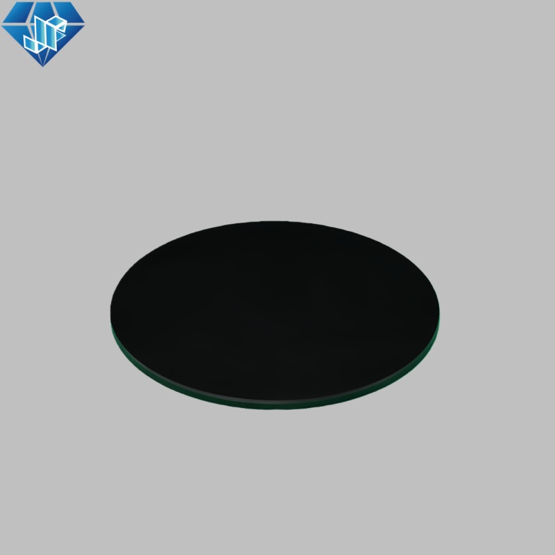
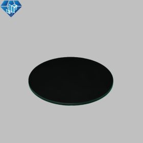
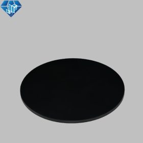
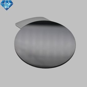
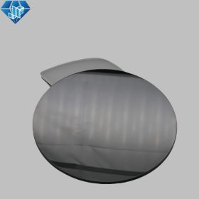
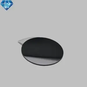
Precision ground SiC substrate ready for final optical polishing.
Why Modern Optics Demand Silicon Carbide (SiC)
Engineers in the semiconductor and aerospace sectors are rapidly transitioning to SiC. While traditional glass is stable, it is brittle and heavy. Beryllium is light but hazardous. A Optischer Spiegel aus Siliziumkarbid solves these material limitations through three distinct physical advantages:
1. Superior Specific Stiffness (Stiffness-to-Weight Ratio)
Stiffness drives performance in dynamic systems. Sintered SiC offers a Young’s Modulus of approximately 410-420 GPa, nearly five times that of standard optical glass.
-
The Benefit: This extreme stiffness allows us to machine the back of the mirror into thin, lightweight structures (honeycomb patterns) without sacrificing optical flatness. For laser galvo systems, this means faster acceleration and higher scanning frequencies without mirror deformation.
2. Exceptional Thermal Stability
In high-power laser applications, energy absorption leads to heat. If a mirror warps due to heat (thermal lensing), the beam quality degrades.
-
The Benefit: With a thermal conductivity of ~150 W/m·K (and up to 200 W/m·K for CVD grades), SiC dissipates heat 100 times faster than glass. Combined with a low Coefficient of Thermal Expansion (CTE), our mirrors maintain their precise shape even under intense thermal loads.
3. Atomic-Level Surface Finishing
Hardness is critical for polishing. Because Silicon Carbide is one of the hardest materials on earth, it can be polished to extreme specifications without scratching.
-
The Benefit: We achieve surface roughness (Ra) values lower than 2 nm (Angstrom level) on our optical-grade CVD-coated mirrors. This minimizes light scattering, making them ideal for UV, X-ray, and high-energy laser applications.
Industry Insight: For detailed standards on ceramic mirror testing, references such as ASTM C1161 (Standard Test Method for Flexural Strength of Advanced Ceramics) provide the benchmarks we adhere to.
Technische Spezifikationen: Sintered vs. CVD SiC
We offer two distinct grades of materials to match your budget and optical requirements.
| Eigentum | Einheit | Sintered SiC (SSiC) | Optical Grade (CVD SiC / SSiC+) |
| Dichte | g/cm³ | > 3.10 | > 3.21 |
| Young’s Modulus | GPa | 410 | 420 – 450 |
| Wärmeleitfähigkeit | W/m·K | 120 – 150 | 180 – 250 |
| CTE (20-1000°C) | 10⁻⁶/K | 4.0 | 2.2 – 4.0 |
| Surface Roughness (Ra) | nm | < 30 | < 2 |
| Bending Strength | MPa | 400 | 500+ |
Advanced Manufacturing & Lightweighting Capabilities
Producing a Optischer Spiegel aus Siliziumkarbid is not just about material; it is about precise shaping.
1. Near-Net Shaping & Green Machining
Before the sintering process, we utilize CNC machining on the “green body” (unfired ceramic). This allows us to create complex honeycomb backing structures or open-back designs. This process reduces the mirror’s mass by up to 60-70% while maintaining structural rigidity—critical for reducing payload weight in aerospace satellites.
2. Reaction Bonding & Sintering
Our vacuum sintering process ensures fully dense materials with no open porosity. For applications requiring zero porosity, we apply a Chemical Vapor Deposition (CVD) SiC layer, which provides a flawless surface for optical coating.
3. Precision Lapping & Metrology
Our facility is equipped with interferometers to verify surface flatness (Ebenheit) to $\lambda/10$ or better. We ensure every mirror meets the strict Wavefront Error requirements of your optical design.
Applications of High-Performance SiC Mirrors
Our substrates are currently deployed in some of the most demanding industries globally:
-
Semiconductor Lithography: Wafer chucks and positioning mirrors that require zero thermal expansion during nanometer-level processing.
-
Laser Scanning & Processing: High-speed galvanometer mirrors for laser marking, cutting, and additive manufacturing (3D printing).
-
Astronomy & Aerospace: Telescope mirrors for earth observation satellites where lightweighting and thermal shock resistance are paramount.
-
Synchrotron & X-Ray Optics: Where surface smoothness must be at the atomic level to prevent beam degradation.
Anpassung & Kontakt
We specialize in lightweight designs, including honeycomb-backed mirrors to reduce mass.
Ready to upgrade your optics?
Please Contact Jifeng Ceramics today for a quote on your custom optical components.