 Цзифэн Керамика

A wafer arriving at the transfer robot has already undergone many expensive process steps. The ceramic arm that carries it is cheap in comparison, but a saggy blade, a shedding surface or a material that can’t take the chamber temperature can still scrap the wafer. There are five checks to selecting a ceramic arm, also referred to as a ceramic end effector or wafer handling arm: process conditions, материал, wafer contact, geometry and cleanliness. Get those right and the rest is for the most part paperwork.
What a Ceramic Arm Does in a Wafer Handling System
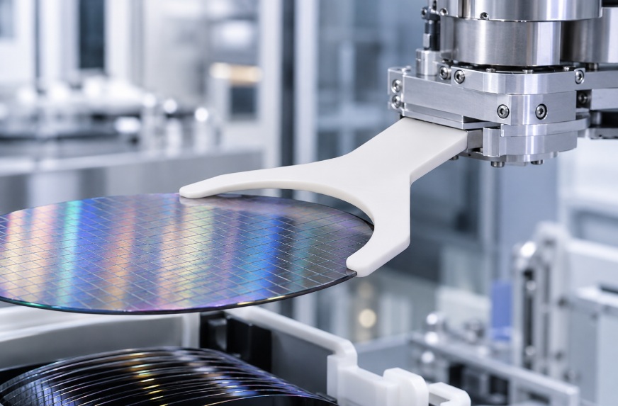
The blade or fork on a wafer-handling robot is known as a ceramic arm. The only thing that touches the wafer as it moves is the device that shuttles wafers between cassettes, transfer chambers and process chambers.
Why Ceramic and Not Metal or Plastic
Metals and polymers are subject to damage from heat, chemicals and frequent contact, and can also introduce contamination. The standard answer is ceramics. Kyocera’s handling arms, например, are made of alumina or silicon carbide and are marketed as resistant to temperature, химикаты, thermal shock, and low friction. Similar arguments are made in Axcelis patent filings on ceramic end effectors which are described as light, relatively low cost and contaminant-free for high-temperature thermal processing, with alumina preferred and silicon carbide an alternative.

Start With Your Process Conditions, Not the Material
Material comes second. The conditions the arm will see decide which materials are even candidates.
Температура
An arm moving wafers near ambient temperature has different needs than an arm entering a thermal process chamber. Thermal shock resistance and thermal conductivity are at the top of the list when repeated heating and cooling are concerned.
Cleaning chemicals
Первый, check chemical resistance and surface stability (in case the arm is exposed to corrosive process chemistry or aggressive cleaning).
Wafer Size, Speed, Atmosphere
Bigger wafers require longer arms and faster cycles mean every gram counts. Also note if the arm operates in vacuum or atmosphere as this affects any internal vacuum lines.
глинозем против. Карбид кремния: Choosing the Right Material
Short Answer
If cost is a factor, alumina is the material of choice for wafer handling. Silicon carbide is the next level when heat and thermal cycling are the dominant factors. According to one ceramics supplier’s comparison, alumina has a thermal conductivity of 20-35 W/m·K compared with about 120-200 for silicon carbide. Silicon carbide is more expensive and more difficult to machine.
Material Comparison
| Свойство | глинозем | Карбид кремния | Цирконий |
| Чистота | ≥99,5% | ≥99,5% | ≥99,9% |
| Плотность | 3.8-3.9 г/см³ | 3.1-3.2 г/см³ | 6.05 г/см³ |
| Long-term temperature (JiFeng) | 800°С | 1600°С | 1200°С |
| Typical thermal conductivity | 20-35 Вт/м·К | 120-200 Вт/м·К | 2-3 Вт/м·К |
| Seen in published wafer-handling designs | Да | Да | Confirm with supplier |
Чистота, density and temperature figures come from JiFeng’s product page. Thermal conductivity is a typical range from the supplier comparison listed under Sources.
When Does Each Material Make Sense
Use alumina for ambient/moderate temperature transfer where cost and availability are important. Choose silicon carbide for severe thermal duty or when low weight and high stiffness are important. Цирконий is on JiFeng’s list, but it is not the standard wafer-handling material in the designs cited above, so confirm the application with the supplier before specifying it.
Design Details That Decide Real-World Performance
Wafer Contact and Gripping
One design has a vacuum channel through the ceramic body and support pads with vacuum orifices on the fingers to hold the wafer without damaging its surface. Ask how many contact points there are. Ask what the pads are made of, and how they are replaced. Whichever method is used.
Геометрия, Thickness and Stiffness
A long, thin blade can droop, which is a problem if the wafer has to slide into a narrow slot. Hollow, lightweight structures cut mass but need careful design. JiFeng’s product page lists hollow lightweight designs among its custom options.
Surface Finish and Mounting
Ask for the surface roughness and edge chamfer for the material you have chosen. JiFeng’s table gives different Ra values for alumina, zirconia and silicon carbide so one figure will not cover all three. Окончательно, verify the mounting interface and arm weight with the payload and inertia limits of the robot.
Чистота, Static and Verification
Particles and Static Control
The two quiet failure modes are static and particle shedding. Alumina is usually an electrical insulator, so don’t expect it to bleed off static; request resistivity data or a static-control solution.
What Evidence to Request
Ask for evidence, not adjectives: dimensional and flatness inspection report, roughness measurements, material certificate. ИСО 14644-1 provides a classification for the cleanliness of cleanroom air . SEMI E78 provides guidelines for electrostatic discharge and attraction control in semiconductor equipment . См. также статью ЦзиФэна. quality and testing страница.
Custom Ceramic Arms: What to Prepare for a Quote
RFQ Checklist
- Wafer size and thickness
- Drawing with tolerances and flatness requirement
- Process temperature, chemicals and atmosphere
- Gripping method: пустой, edge or support pads
- Preferred material, if any
- Quantity and inspection requirements
How JiFeng Can Help
ЦзиФэна ceramic arm lists custom structures including multi-axis joints and hollow lightweight designs, plus surface treatments, and shows ISO 9001 for its alumina and silicon carbide arms. Ask for the certificate and a drawing review with your quote.
A Simple Way to Decide
Work in this order: conditions, материал, contact method, геометрия, then verification.
Alumina or silicon carbide? Alumina for balanced cost and general transfer; silicon carbide for heavier thermal duty.
Can a ceramic arm be customized? Да. Send drawings and process details.
What should I send for a quote? Wafer size, допуски, условия эксплуатации, gripping method and quantity.
To discuss a custom ceramic arm for your semiconductor equipment, запросить цену.
