 JiFeng-Keramik

In the extreme environment of semiconductor manufacturing—high temperatures, aggressive plasma, ultra-high vacuum, and ultra-clean requirements—equipment components must deliver exceptional reliability. Among advanced ceramics such as silicon carbide (SiC), Aluminiumnitrid (AlN), Siliziumnitrid (Si₃N₄), and yttria (UND₂ODER₃), Aluminiumoxidkeramik (Al₂O₃) consistently account for approximately 45% of precision ceramic components used in semiconductor equipment. This makes alumina ceramics the most widely adopted ceramic material across etching, Ablagerung, Polieren, and wafer-handling systems.
The dominance of alumina ceramics is no accident. It stems from an outstanding balance of performance, cost-effectiveness, and manufacturing maturity. This article explains why alumina ceramics have become the preferred choice in Halbleiterausrüstung through four key perspectives: material properties, real-world applications, competitive comparison, and future trends.
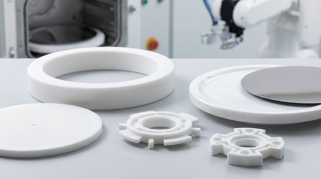
Core Performance Advantages of Alumina Ceramics in Semiconductor Equipment
Semiconductor processes demand materials that combine plasma resistance, Hochtemperaturstabilität, excellent electrical insulation, low particle generation, and dimensional precision. Hochreine Aluminiumoxidkeramik (typically ≥99.5% purity, with etching-grade materials reaching 99.8% or even 4N/99.99%) meet these requirements exceptionally well.
Hervorragende elektrische Isolierung
High-purity alumina ceramics offer volume resistivity of 10¹⁴–10¹⁶ Ω·cm and a dielectric constant of approximately 9–10 with very low dielectric loss. These properties make alumina ceramics ideal for electrode holders, Isolierringe, isolation components, and electrostatic chucks (ESC), effectively preventing leakage current, electrostatic discharge, and electromagnetic interference.
Outstanding High-Temperature Stability and Dimensional Accuracy
With a melting point near 2050°C, alumina ceramics can operate continuously at 800–1600°C in vacuum or heated environments. Their relatively low coefficient of thermal expansion (approximately 7–8 × 10⁻⁶/°C) ensures micron-level dimensional stability during rapid thermal cycling in CVD and ALD processes, minimizing thermal stress and deformation.
Superior Chemical and Plasma Corrosion Resistance
In plasma etching chambers, components face highly corrosive halogen-based plasmas (fluorine and chlorine chemistries). High-purity alumina ceramics demonstrate excellent resistance to acids, Basen, and reactive plasmas. Their etch rate is significantly lower than that of quartz, and they generate minimal particles—critical for maintaining high wafer yields.
High Hardness and Mechanical Strength
Alumina ceramics possess a Mohs hardness close to 9 (an zweiter Stelle nach Diamant) and flexural strength typically ranging from 350–550 MPa. This combination delivers outstanding wear resistance for polishing plates, vacuum chucks, robotic arms, and gas distribution rings that experience continuous mechanical stress and friction.
High Cleanliness and Ultra-Low Contamination
Semiconductor-grade alumina ceramics are manufactured with strict control of metallic impurities (Na, K, Fe, Ca, usw.). Surfaces can be finished to extremely low roughness, resulting in near-zero particle release in cleanroom environments such as lithography and metrology tools.
Decisive Cost and Process Maturity Advantages
Compared with SiC and AlN, alumina ceramics benefit from abundant raw materials, mature sintering and precision machining processes, and high production yields. This superior cost-performance ratio enables widespread use of alumina ceramic components throughout semiconductor equipment rather than limiting them to niche high-end applications.
These combined attributes explain why alumina ceramics remain the foundational ceramic material in semiconductor manufacturing equipment.
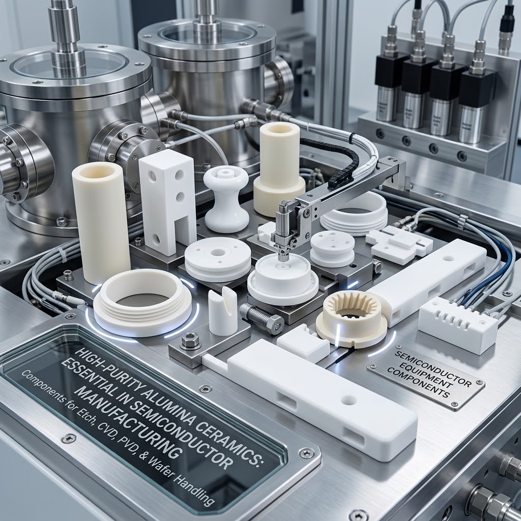
Key Applications of Alumina Ceramics Across Semiconductor Processes
Alumina ceramics are used extensively throughout the semiconductor fabrication line. Major applications include:
Plasma Etching Equipment
- Chamber liners and protective components that resist plasma erosion
- Focus rings, Gasdüsen, gas distribution plates, Isolierringe, and covers
High-purity alumina ceramics often deliver several times the service life of quartz equivalents while reducing particle contamination.
Deposition Processes (CVD, PVD, ALD)
- Susceptors (heater bases), electrostatic chucks (ESC), and ceramic heaters
- Gas distribution plates and chamber structural parts
These components require high-temperature stability, uniform thermal conductivity, and precise dimensional control—areas where alumina ceramics excel.
Chemical Mechanical Polishing (CMP)
- Polishing plates, pad-conditioning platforms, vacuum chucks, and transfer arms
The exceptional hardness and abrasion resistance of alumina ceramics ensure long service life under continuous mechanical friction and chemical exposure.
Wafer Handling and Other Critical Components
- Ceramic robotic end effectors, vacuum chuck bases, thermal insulation pads, and sensor housings
Alumina ceramics provide the optimal combination of electrical insulation, Verschleißfestigkeit, low particle generation, and structural strength. From a total cost of ownership perspective, alumina ceramic robotic arms often outperform silicon carbide alternatives.
In advanced packaging, alumina ceramic substrates (including DBC substrates) continue to be widely used thanks to their insulation performance, mechanical reliability, and cost advantages.
Comparison with Other Advanced Ceramics: Why Alumina Ceramics Dominate
| Material | Key Strengths | Main Limitations | Typical Role in Semiconductor Equipment |
| Aluminiumoxid (Al₂O₃) | Balanced properties, low cost, ausgereifter Prozess | Mäßige Wärmeleitfähigkeit; limited lifetime in extreme fluorine plasmas | ~45% market share – structural & protective components |
| Siliziumkarbid (SiC) | Hohe Wärmeleitfähigkeit, extreme stiffness & Verschleißfestigkeit | High cost, difficult machining | Precision stages, Führungsschienen, high-stiffness parts |
| Aluminiumnitrid (AlN) | Excellent thermal conductivity, CTE close to silicon | Expensive, relatively weaker plasma resistance | High-power heat dissipation, ESC bases |
| Yttria (UND₂ODER₃) | Superior resistance to fluorine plasma | High cost, mainly used as coatings or niche parts | Premium etch chamber protection coatings |
| Siliziumnitrid (Si₃N₄) | Hohe Festigkeit, Zähigkeit, Thermoschockbeständigkeit | Intermediate cost and machinability | Bearings and structural components |
Alumina ceramics do not lead in every single performance metric. Jedoch, they deliver the best overall balance of “sufficient performance + controllable cost + mature supply chain.” Most semiconductor equipment applications do not require the absolute highest specification material in every location—alumina ceramics cover the broadest range of needs effectively.
Technical Requirements and Future Development Trends
Semiconductor equipment demands high-purity alumina ceramics: general structural parts typically require ≥99.5% purity, while etching-grade components often need ≥99.8% or even 99.99% (4N) transparent or translucent grades. Fine-grained microstructure, near-zero porosity, and ultra-precise surface finishing have become standard requirements.
Blick nach vorn, key trends include:
- Higher purity and nano-scale grain control to further reduce contamination risk for advanced nodes
- Functional composites and coatings (z.B., alumina base + yttria plasma-resistant coatings) that combine cost efficiency with extended lifetime
- Accelerated domestic substitution: precision ceramic components account for more than 10% of semiconductor equipment cost, creating significant opportunity for high-purity alumina ceramic parts
- Expanding applications in third-generation semiconductor (SiC, GaN) Ausrüstung, advanced packaging, and Mini/Micro-LED manufacturing
Abschluss
Alumina ceramics have become the most widely used ceramic material in semiconductor equipment because they deliver “good enough” comprehensive performance at a “sufficiently low” cost supported by a fully mature supply chain. From etch chamber liners and heating platforms to polishing plates and wafer-handling arms, alumina ceramic components quietly underpin process stability and wafer yield.
As the semiconductor industry advances toward more complex processes and higher-performance equipment—and as domestic equipment and materials substitution accelerate—the importance of high-purity alumina ceramics will only continue to grow. They remain both a proven foundational material and an evolving critical enabler for next-generation semiconductor manufacturing.
