 吉峰陶磁器
吉峰陶磁器

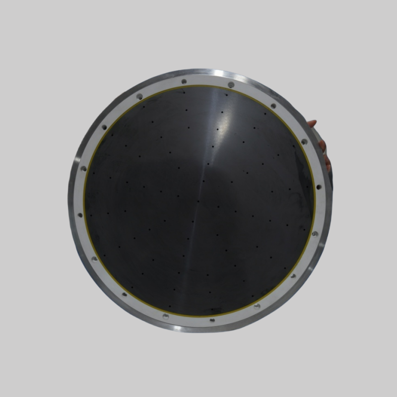
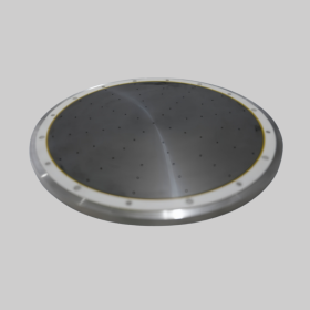
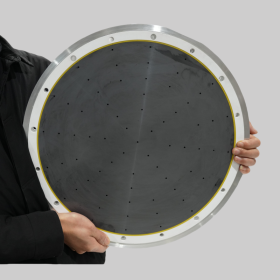
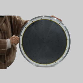
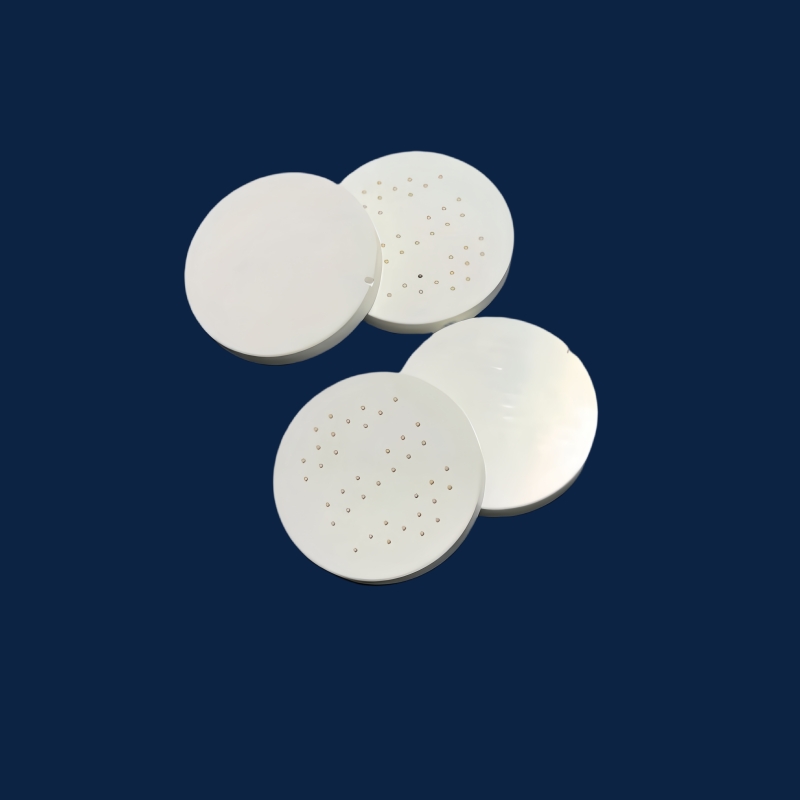
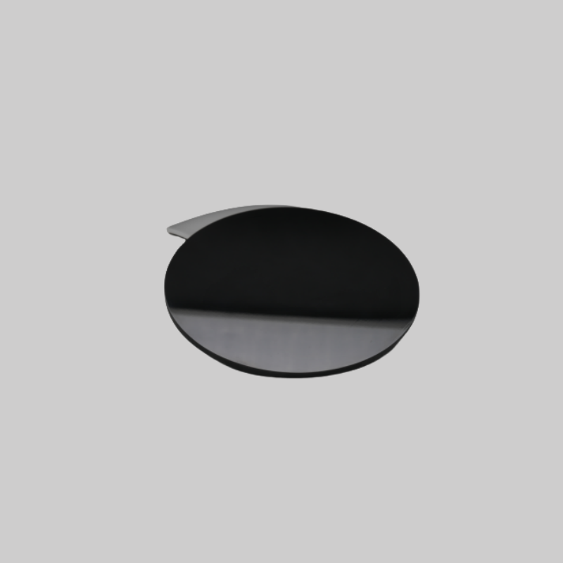
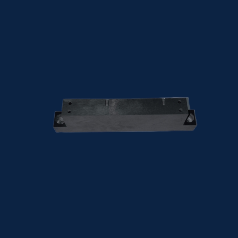
主な利点 Porous Ceramic Vacuum Chuck
極端な温度耐性
Long-term working temp 1600°C; thermal shock ΔT ≥ 500°C.
Precision micro-porous adsorption
気孔率 30~70%, pore size 1–50 μm; vacuum adsorption ≥ 0.08 MPa for ultra-thin wafers.
腐食 & 耐摩耗性
Resists pH 1–14 & plasma erosion; HV10 2200–2800; service life 3× of graphite chucks.
Ultra-high flatness
≤ 0.005 mm after precision grinding.
Key Applications Of Porous Ceramic Vacuum Chuck
1.半導体 & エレクトロニクス
- Wafer bonding / temporary bonding: flatness ≤0.005 mm for 12-inch wafer thinning.
- Lithography thermal management: temperature fluctuation ≤±0.1°C.
2.Photovoltaic & 新エネルギー
- PERC/TOPCon solar cell sintering furnace: 1600℃, breakage rate ≤0.01%.
- SiC epitaxial tray: metal impurity ≤1 ppm for MOCVD/MBE.
3.Laser & 精密加工
- High-power laser cutting chuck: resists laser ablation ≥1 kW/cm².
- 3D printing substrate: porous ventilation reduces powder adhesion.
4. 高温産業機器
- Sintering furnace setter: 耐クリープ性, load ≥50 kg/m² at 1600°C.
- Vacuum brazing fixture: resists Ag-Cu-Ti solder; reusable ≥1000 cycles.
JiFeng セラミックスカスタマイズサービス
Pore structure
uniform / gradient / directional channels for vacuum/gas control.
Surface treatment
CVD SiC coating, anti-oxidation SiO₂/Al₂O₃ coating.
Dimensions
diameter φ100–φ600 mm, thickness 5–50 mm; rectangular / special shape.
Cost advantage
40–60% lower than imported brands.